Simple Multi-Cycle Central Processing Unit (CPU)
Simple Multi-Cycle Central Processing Unit (CPU)
INTRODUCTION
A simple multi-cycle central processing unit (CPU) shown in Figure 1 designed and implemented, that has a data-path unit and a hard-wired control unit which can process 8-bit data through various register transfers and ALU operations over a common 8-bit bus. There were three parts to this project. In the first phase, we would have to understand the description of the block diagram. The second phase involves the design and implementation of the major components of the simple multi-cycle CPU such as register file, arithmetic logic unit (ALU) and a counter in our default software Multisim. We used “sub-circuits” to make your design look cleaner and easy to deal with. In the final phase we designed the control logic and made its implementation. After all of this part we had the formal definition of our simple multi-cycle central processing unit design (CPU).
Figure 1. Block diagram of a simple multi-cycle 8-bit processor
THEORY
The digital system can perform different operations in each clock cycle, mainly governed by the control signals of the control logic. Each instruction can be loaded and stored in the instruction register (IR) using the 8-bit format “IIXXXYYY”, where II represents the instruction type or so called OP code (2 bits, denoted as OP 0 and OP 1), XXX gives the Rx register address (using simple binary addressing (x)2), and YYY gives the Ry register address ((y)2). The CPU starts executing the instruction on the DIN input when the Run signal is asserted and the CPU asserts the Done output when the instruction is finished executing.
Figure 2. The set of control signals asserted for each instruction and time step
Figure 3. The instructions of the processor
TRUTH TABLE AND KARNOUGH MAPS
Table 1. Truth table for the control circuit
Table 3. Karnough Map of Rxout
Table 4. Karnough Map of Ryout
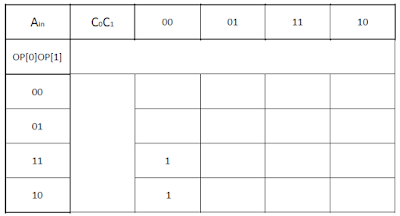
Table 5. Karnough Map of Ain
Table 6. Karnough Map of Bin
Table 7. Karnough Map of Bout
Table 8. Karnough Map of Asen
Table 9. Karnough Map of Din
Table 10. Karnough Map of Done
Minimization of Karnough maps:
Rxin = OP[0]’.C1’.C0’ + P[0].C1’.C0
Rxout = OP[0]’.C1’.C0’
Ryout = OP[0]’.OP[1]’.CO’.C1’ + P[0].C0’.C1
Ain = OP[0].C1’.C0’
Bin = OP[0]’.C1.C0’
Bout = OP[0].C1’.C0
Asen = OP[0].OP[1].C0.C1’
Din out = OP[0]’.OP[1].C0’.C1’
Done = OP[0]’.C1’.C0’ + P[0].C1’.C0
DISCUSSION
In this project we learned to use Logisim program and implementation of instruction type. We used Logisim program because it is easier than others. The first design had not a control logic and we did not know how could implement it. Than we understood basic structure of control logic and we made a control logic. The most challenging spot was enable. Because when we did enable part, we could not choose a register in first time. We created MUX and we connect the Rxin and the output of MUX in and gate, and we did this.
Figure 4. Design of simple multi-cycle CPU


Comments
Post a Comment